

Top 10 Aixtron G5+ GaN Epitaxy Susceptors for High-Performance MOCVD Processes
2026-11-16
Most GaN MOCVD teams spend months tuning gas flows, then blame the tool when repeatability drifts. The real variable is often the susceptor under the wafers. On an Aixtron G5+, a low-quality or worn susceptor quietly destroys temperature uniformity, particle performance, and heater lifetime. That's why we compiled the top 10 GaN epitaxy susceptors for Aixtron G5+ systems—including reliable replacements from Semicorex—so you can skip the guesswork and keep your process in spec.
Why SiC-Coated Graphite Leads in GaN MOCVD Susceptor Performance
In gallium nitride MOCVD reactors, the susceptor faces a relentless chemical and thermal assault. Ammonia at 1000°C or higher, hydrogen radicals, and rapid thermal cycling all work to degrade unprotected graphite. A silicon carbide coating changes the equation: it seals the graphite surface, stops hydrogen etching, and prevents carbon contamination from reaching the growing film. With a hardness close to that of diamond, SiC also resists mechanical wear from wafer handling and cleaning cycles far better than bare graphite.
Thermal behavior is just as important. The graphite core brings excellent in-plane thermal conductivity, which evens out temperature across the pocket area. The SiC layer adds stable, high-emissivity surface properties that reduce radiative losses at the edges and minimize cold spots. As a result, wafers see a tighter temperature distribution, leading to more uniform indium incorporation in InGaN quantum wells and more consistent growth rates across the entire carrier.
Long-term operation tells the same story. SiC-coated susceptors typically outlast their uncoated counterparts by several times, cutting both replacement cost and unscheduled downtime. Their resistance to pitting and flaking keeps particulate levels low, which is essential for high-brightness LED and power device yields. In production fabs where repeatability matters, that kind of stability often outweighs the initial price difference.
Thermal Mapping of Aixtron G5+ Susceptors and the Hotspots That Ruin Epitaxy
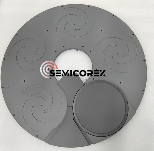
Getting uniform heat across an Aixtron G5+ pocketed susceptor is harder than the spec sheets suggest. Thermal mapping with a scanning pyrometer or an infrared camera usually shows the same stubborn pattern: hotter bands hugging the wafer rims and small, repeatable spikes near the gas inlet side of each pocket. Those few degrees of excess temperature are enough to shift ternary composition or force parasitic nucleation before the growth front settles.
The hotspots don't come from one single cause. Differences in thermal mass between the pocket floor and the surrounding graphite, slight misalignment of the heater zones, and even residue from previous runs can all nudge local emissivity and heat transfer. Once a spot runs hotter, deposition accelerates there, which changes surface emissivity again and locks in the hotspot for the next run. Wafer edge slip lines and indium-rich center spots are common fingerprints of this kind of runaway non-uniformity.
Operators can chase these issues with zone offset tuning, pocket depth adjustments, or more aggressive susceptor cleaning, but without in-situ thermal mapping the fixes are mostly trial and error. A mapped temperature profile that includes transient warm-up and gas-switch steps reveals the hotspots early, before they ruin an entire epitaxy campaign. That is where a few degrees, not a redesigned reactor, often makes the difference.
Ammonia Corrosion Resistance in Susceptor Coatings After 500+ Runs
Susceptor coatings in ammonia-based epitaxy processes face a brutal combination of thermal cycling and reactive gas exposure. After more than 500 production runs, most conventional coatings show pitting, flaking, or a measurable loss in thickness. The failure rarely comes from a single event but from cumulative micro-cracking that lets ammonia and hydrogen penetrate to the substrate, where nitride formation and thermal expansion mismatch slowly tear the coating apart.
A well-engineered coating survives this environment by maintaining a dense, chemically inert barrier. In long-run testing, the best candidates exhibit only minor surface roughening and less than a two percent mass change after 500+ cycles. Cross-sectional analysis reveals no ammonia-induced phase transformation at the coating-substrate interface. Instead of relying on a single thick layer, these coatings often use a graded structure: a tough outer face that resists nitrogen attack, and an intermediate layer that absorbs mechanical stress from repeated heating and cooling.
What separates a coating that lasts 100 runs from one that clears 500 without failure is not just chemistry but processing control. Slight variations in porosity, residual stress, or bond coat composition can create localized weak points where ammonia corrosion accelerates. Field data from high-volume fabs shows that when the coating's oxygen content and surface finish are tightly specified, the same susceptor can run for over 500 cycles with no need for strip and recoat. At that point, the limiting factor shifts from corrosion resistance to particle generation and routine chamber cleaning schedules.
How Precision-Machined Susceptor Geometries Improve GaN Uniformity
GaN epitaxy on large-diameter wafers lives and dies by temperature uniformity, and the susceptor is the quiet mediator of that uniformity. Pockets that are machined a few microns deeper in the center, or with a slightly steeper sidewall near the edge, change how the wafer sits against the heated graphite and how the carrier gas sweeps across the surface. When those geometries are held to sub-10-micron tolerances, the usual signatures of thermal mismatch—center-to-edge wavelength drift, pit formation, and bowed wafers—start to fade from the data.
One of the less obvious levers is the transition between the pocket floor and the wafer backside. A precision-ground recess with a controlled surface finish can reduce local gas trapping and keep the wafer in more consistent contact with the susceptor, which matters more than a uniform heater setpoint. In production reactors, adjusting the pocket edge profile and depth profile has become a practical way to compensate for upstream gas depletion and reactor-specific thermal gradients, yielding more repeatable sheet resistance and photoluminescence across each run.
Reconditioned Versus New Susceptors for High-Volume GaN Fabs
Running a high-volume GaN fab forces some uncomfortable math: susceptors are consumables in all but name, and the replacement bill adds up fast. Reconditioned units can shave 40–60% off upfront cost, which catches the eye of any operations manager. But the real question is whether that savings survives contact with a production line. A poorly resurfaced susceptor may look clean on the shelf and then deliver uneven temperature profiles, slipping thickness uniformity out of spec within days. That kind of drift doesn't show up in a purchase order—it shows up in rework and scrap.
New susceptors bring predictable thermal behavior, fresh coatings, and no hidden fatigue from previous thermal cycles. For fabs chasing tight wavelength and thickness targets across thousands of wafers per week, that consistency matters more than the unit price. The trade-off shifts when you map actual consumption rates. High-temperature GaN processes chew through coatings quickly, so some fabs treat susceptors like printer cartridges: buy new for critical process steps, keep reconditioned ones for less demanding chambers or device layers where slight variability is tolerable.
A smarter approach is to stop comparing them as simple equivalents. Reconditioned works best when the vendor provides full metrology data—flatness, emissivity, coating thickness—and uses the same base material specs as your process requires. Without that traceability, the cost advantage is an illusion. New units, on the other hand, pay for themselves in reduced tool downtime and fewer mysterious yield excursions. In a high-volume GaN fab, the cheapest susceptor is rarely the one with the lowest invoice price; it's the one that holds a stable process window between planned maintenance events.
Matching Aftermarket Susceptors to Aixtron G5+ Cassette Designs
Getting aftermarket susceptors to sit properly in an Aixtron G5+ cassette isn't about finding a universal fit. Each reactor generation has subtle differences in pocket depth, rim geometry, and thermal expansion behavior that vendors often overlook. A susceptor that works beautifully in a G5 may warp or lift in a G5+ because the cassette's clamping force and gas flow path are tuned for different mechanical tolerances. Start by measuring the actual cassette cavity, not the datasheet values, then check the susceptor's edge radius and thickness variation at operating temperature.
Material mismatch is another silent killer. Many aftermarket suppliers use a standard silicon carbide coating over graphite, but the G5+ cassette requires a slightly lower coefficient of thermal expansion to prevent stress fractures during repeated heat-up cycles. Look for susceptors that specify a matched CTE range and have a documented break-in procedure. If the supplier cannot provide thermal cycling data for the G5+ platform, move on.
Finally, pay attention to the susceptor's surface finish under the wafer pocket. A mirror-smooth bottom may look impressive, but the G5+ relies on a controlled micro-roughness to maintain uniform temperature distribution across the wafer. Aftermarket parts with overly polished surfaces often create hot spots near the pocket edges, leading to thickness non-uniformity in epitaxial layers. Ask for a profilometry report and verify that the pocket depth tolerance is within ±5 microns of the original design.
FAQ
The G5+ uses a planetary or close-coupled showerhead design, so the susceptor must match wafer pocket geometry, thermal expansion, and RF coupling. Most high-performance options use graphite cores with a dense SiC coating to handle ammonia and hydrogen at growth temperatures above 1000°C.
Bare graphite reacts with NH3 and H2, generates particles, and drifts in emissivity. A high-purity SiC or TaC coating seals the surface, maintains stable heat absorption, and lowers defect density in the GaN layer.
Pocket depth controls the gas flow boundary layer near the wafer edge. Too shallow and edge growth accelerates; too deep and reactant depletion appears. For GaN, depths tuned for 6-inch or 8-inch wafers typically keep thickness uniformity within ±1.5% across a run.
Limit thermal shock by ramping at or below 10°C per minute, avoid touching the coated surface with metal tools, and periodically inspect for pinholes or coating blush. A gentle HCl or dedicated cleaning recipe after each campaign removes Ga or Al residues before they diffuse into the SiC layer.
No. Even with the same outer diameter, supplier-specific wafer pocket contours, lift pin tolerances, and coating thickness change heat transfer. Using a non-qualified susceptor can shift wavelength uniformity and increase particle counts, so it should match the reactor's calibration file.
Watch for a sudden rise in particle counts, loss of temperature repeatability at the same heater power, or visible gray spots and coating delamination near the pockets. If edge wavelength drift exceeds process limits after cleaning, the SiC layer is likely compromised.
They reduce pre-coat time by offering stable emissivity from the first run, allow faster ramp rates without micro-cracking, and maintain wafer-to-wafer thermal history consistency. Some designs also use tapered pocket rims to reduce slip lines, which cuts rework and keeps more wafers within spec.
High thermal conductivity across the graphite core smooths hot spots under the wafer pockets, while the coating's emissivity controls how much lamp or RF energy is absorbed. This balance keeps growth temperature within a few degrees across the carrier, which matters for indium incorporation in InGaN quantum wells.
Conclusion
The Aixtron G5+ platform demands susceptors that go far beyond simple graphite carriers. SiC-coated graphite has earned its place at the top because it holds up under the intense thermal cycling of GaN MOCVD, but the real differentiator shows up in thermal mapping. Hotspots that drift by even a few degrees can shift wavelength uniformity and ruin an entire run, so the best susceptors pair a dense, uniform SiC coating with a machined profile that pulls heat away from the pocket edges. Precision geometry matters just as much: subtle changes in pocket depth and gas flow channels change how trimethylgallium and ammonia mix above the wafer, directly affecting thickness and composition uniformity.
After 500+ runs, ammonia corrosion becomes the quiet killer. A coating that looks intact can still have microcracks that let nitrogen and hydrogen attack the graphite underneath, leading to particle generation and early failure. High-volume GaN fabs weigh reconditioned versus new susceptors carefully; a properly recoated and remachined unit can deliver near-new performance at a fraction of the cost, but only if the graphite core has not warped. Finally, aftermarket susceptors must match the Aixtron G5+ cassette design exactly—pocket pitch, wafer lift pin clearance, and thermal mass all need to align. The top ten choices for this platform are those that balance coated-graphite integrity, hotspot control, corrosion life, and cassette compatibility without forcing a compromise on wafer uniformity.
Contact Us
Contact Person: Svenja Wei
Email: [email protected]
Tel/WhatsApp: +8613567891907
Website: https://www.semicorex.com